Latest Research
Accurate measurement of changes inside semiconductors using “light”
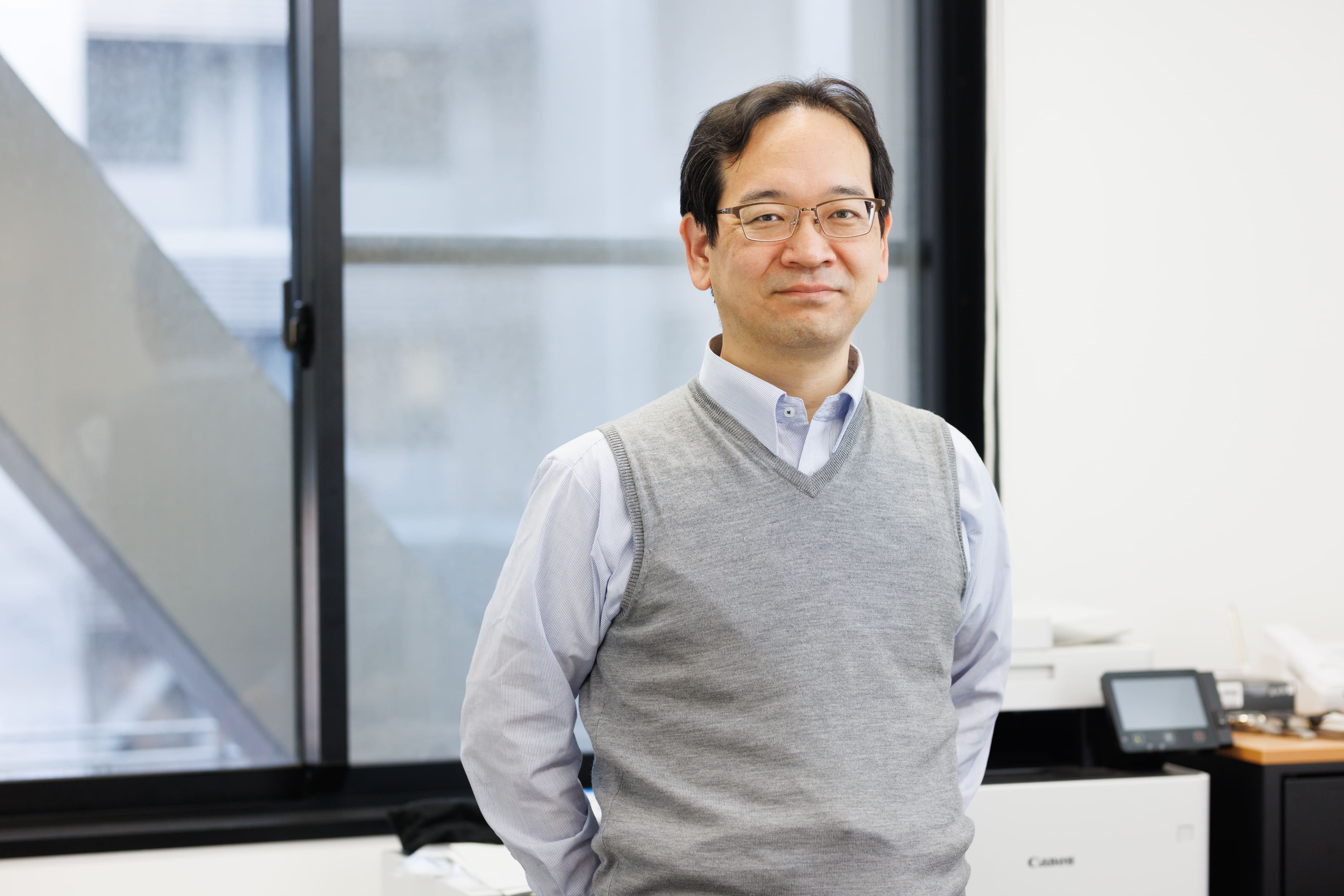
PROFESSOR. Atsutomo Nakamura
 Generally, hard
materials have the property of being brittle and fragile. Ceramics and semiconductors are typical of such
materials. We have been working on research to investigate changes in the strength and structure of a
substance, by irradiating the surface of the substance while applying force to it at the micro level which
is smaller than atom and even electron. Our researches are based on the hypothesis that we could freely
change the hardness and strength of a substance just by shedding light on it. The latest achievements were
published in the online version of the American scientific journal “Nano Letter” in February 2021.
Generally, hard
materials have the property of being brittle and fragile. Ceramics and semiconductors are typical of such
materials. We have been working on research to investigate changes in the strength and structure of a
substance, by irradiating the surface of the substance while applying force to it at the micro level which
is smaller than atom and even electron. Our researches are based on the hypothesis that we could freely
change the hardness and strength of a substance just by shedding light on it. The latest achievements were
published in the online version of the American scientific journal “Nano Letter” in February 2021.
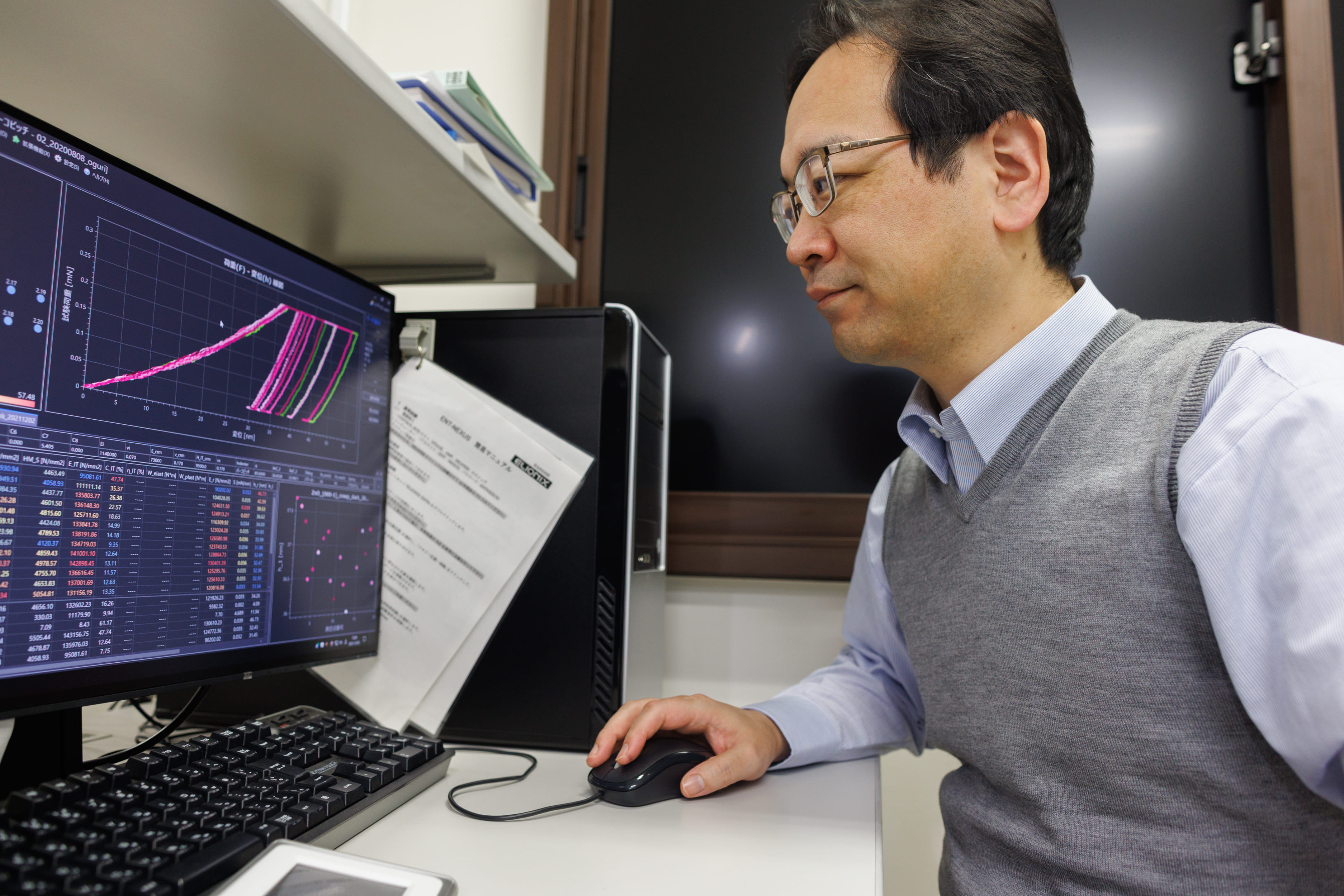
Three years ago, in May 2018, our research group reported that the inorganic semiconductor crystals would acquire the plasticity (ability to change shape) of metallic materials and would be less likely to break, when placed in a completely dark room with no light. This time, we have further advanced the research and developed the precise measurement method; we have improved the “indentation method,” which measures the strength by pressing the pointed tip of a measuring device against a substance, and have successfully established an “optical indentation method,” in which “light” is simultaneously incident on the sample and the inside of a substance is measured on a nanoscale together with its “force.”
In other words, we have demonstrated that visible light from the outside can change the nanoscale region inside the substance without changing the structure of the substance itself.
Deepening research by improving the accuracy of nanoscale measurement method
 One of the
achievements of this experiment was to clarify the relationship between light and changes in physical
properties. “Wrinkles” occur when pressure is applied to the inside of crystals, such as semiconductors, to
deform them. In this experiment, it was found that the strength of the crystal is determined by how the part
called “Wrinkles (Dislocation)” moves. In other words, it became clear that the strength of a substance can
be controlled by using light. This has resulted in even more “light” being shed on the study of changes in
the strength of materials caused by the motion of electrons and photons smaller than atoms.
One of the
achievements of this experiment was to clarify the relationship between light and changes in physical
properties. “Wrinkles” occur when pressure is applied to the inside of crystals, such as semiconductors, to
deform them. In this experiment, it was found that the strength of the crystal is determined by how the part
called “Wrinkles (Dislocation)” moves. In other words, it became clear that the strength of a substance can
be controlled by using light. This has resulted in even more “light” being shed on the study of changes in
the strength of materials caused by the motion of electrons and photons smaller than atoms.
Furthermore, it brought great achievements to the measurement method itself. It has been well known that light causes changes in the strength of semiconductors, but it has not been possible to realize a method that can accurately measure the moves of “Wrinkles” on a nanoscale. By realizing the method mentioned above, it has become possible to accurately evaluate the strength of a substance when it is exposed to light, not limited to semiconductors. This is also one of our big achievements this time.
Currently, we are collecting experimental data using the original device for which we reported the results. Our future goal is to contribute to research on increasing semiconductor productivity by providing detailed information on the strength of semiconductors that have not been studied from the perspective of the effects on light. At the same time, as an important mission assigned to me, I would like to further improve the accuracy of measurement technology.
Advances in such research will ultimately lead to expanding the possibilities of manufacturing. You don’t have to spend a lot of time searching for alternative materials without any special processing on the material. In other words, it may be possible to realize a future in which existing materials can be used to produce more robust and lightweight mobiles and vehicles with less energy, without cost and effort.
Aiming for “game change” by fusing different fields
In the first place, investigating the strength of substances is in the field of mechanical engineering or materials engineering, and research related to the effects of light and electrons is in the field of applied physics or electrical engineering. I can say that my specialty is a cross-disciplinary research area that goes back and forth between different disciplines. I myself majored in the mechanical engineering field in the undergraduate and master’s courses, but chose the materials field in the doctoral course. Also, since that time, I have been studying fusion fields including the field of applied physics. I feel that the pursuit of fusion fields between different disciplines from my student days to the present has led to the formation of my research style today.
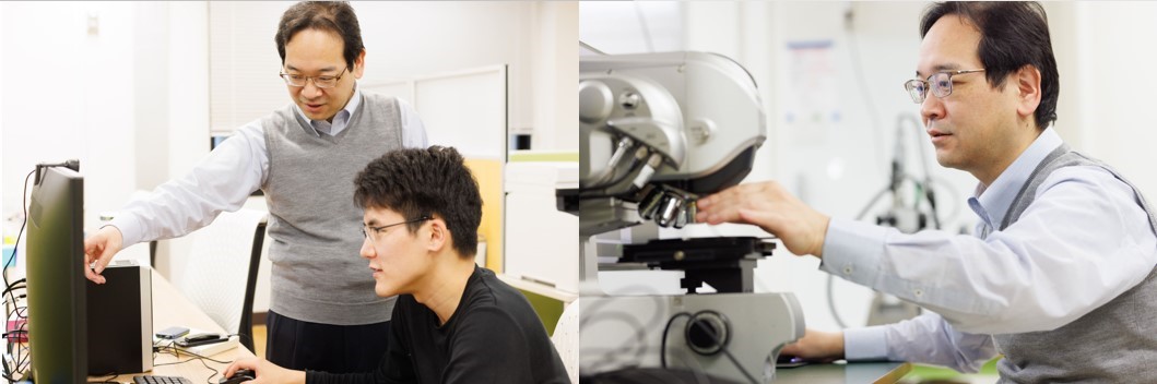
This is in line with the policy of the School of Engineering Science/ the Graduate School of Engineering Science, Osaka University. In the future, I would like to continue my research from both aspects of the strength and structural properties, and at the same time, I would like to take the stance of making and analyzing the devices to evaluate them myself.
Considering the future research environment, the promotion of remote research will further speed up and improve the efficiency of research. It is necessary to pursue ingenuity, such as pursuing uniqueness of research and creating original devices, so as not to be left behind by the global trend.
Research is meaningful only in “the world’s best” or “the world first,” and there is no point in being the first in Japan. Having such a solid understanding of what research is, and focusing on developing young human resources who can compete with the world’s top-level people is also a major role for me in the future. While deepening my research theme, I would like to devote myself to developing world-class human resources as my mission.
By pursuing the unknown properties of substances and materials, it is my ultimate goal as a researcher to bring about “game changes,” which will fundamentally change people’s lives. I won’t stop until that day comes.